Test Wafers
tei Solutions offers 100mm, 150mm, 200mm, and 300mm blanket and pattern wafers for material and tool evaluation including:
- Line and Space
- Hole Pattern
- Al Pad wafers
- Cu Pad wafers
- Others – Please contact us for special structures or materials. Customers can utilize their own mask set if the clean level is acceptable.
φ300mm Patterned Wafer Examples
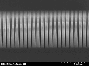
L/S=260/40nm, SiO Etch
Pitch=300nm(6.5:1)
AR=approx.4.5(Depth=190nm)
X-SEM
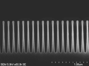
L/S=45/45nm, Si Etch
Pitch=90nm(1:1)
AR=approx.11(Depth=500nm)
X-SEM
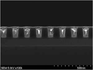
TOP CD(Cu)=approx.80nm,
Low-k Etch
Pitch=160nm(1:1)
Depth=180nm
X-SEM
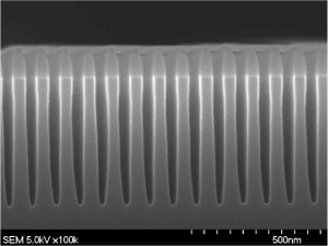
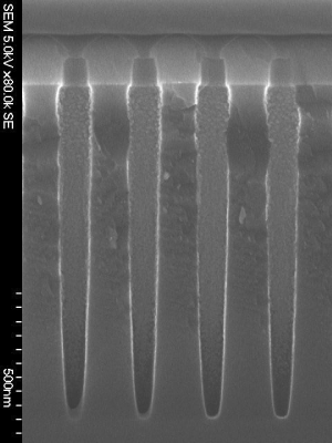
Si L/S Etch
Si Substrate Etching
(Top)L/S=50nm/90nm, Pitch=140nm
Depth=1000nm
X-SEM
Si Hole Etch
(Top)Hole=φ120nm
Depth=1200nm
X-SEM
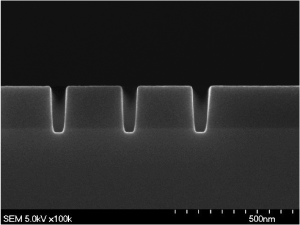
SiO2 L/S Etch
SiO film etching
(Top)L/S=180nm/120nm, Pitch=300nm
Depth=2700nm
X-SEM
φ300mm Blanket Wafer Examples
| Classification | Method | Type or Film | Tickness Range (nm) |
|---|---|---|---|
| SiO | Thermal | RTO | 1〜5 |
| Radical Ox | 2〜11 | ||
| Wet Ox (Batch) | 4〜500 | ||
| CVD | P-SiO2 | 2〜500 | |
| LP-TEOS (Batch) | 10〜700 | ||
| P-TEOS | 10〜2,000 | ||
| HDP | 30〜1,000 | ||
| SiN | CVD | LP-SiN HCD (Batch) | 2〜150 |
| LP-SiN DCS (Batch) | 2〜250 | ||
| P-SiN | 30〜2,000 | ||
| Nitridation | Nitridation | RTN | 1〜5 |
| Gate-nitridation | ─ | ||
| High-K Nitridation | ─ | ||
| a-Si | CVD | a-Si (Batch) | 10〜300 |
| Poly-Si | CVD | Poly-Si (Batch) | 20〜500 |
| SiOC | CVD | P-SiOC (non-porous) | 50〜800 |
| P-SiOC (porous) | 100〜800 | ||
| SiCO | CVD | P-SiCO | 10〜500 |
| SiCN | CVD | P-SiCN | 50〜200 |
| W | CVD | CVD-W | 50〜800 |
| AlCu | PVD | AlCu Sputter | 160〜1,200 |
| Cu | PVD | Cu Sputter | 15〜300 |
| Plating | Cu Plating | 300〜50,000 | |
| TiN | CVD (dense) | CVD-TiN (dense) | 5〜10 |
| Ti, TiN | CVD | CVD-Ti/TiN | Ti 1〜20 TiN 1〜50 |
| Ti, TiN | PVD | Ti/TiN Sputter | Ti 5〜20 TiN 5〜50 |
| Ta, TaN | PVD | Ta/TaN Sputter | Ta 8〜80 TaN 5〜50 |
| Ni, TiN | PVD | Ni/TiN Sputter | 5〜200 5〜130 |
| Resist for Imm ArF | Coater | Only Resist Coat | |
| SOG | Coater | Only SOG Coat | |
| SOC | Coater | Only SOC Coat | |
| Resist for KrF | Coater | Only Resist Coat |
φ200mm – Patterned Wafer Examples
- High Aspect ratio Si hole pattern, Hole size 200nm, AR=40.
- Al Pattern, VIA size 800nm,
- Al Pattern, 0.35micron
- Deep Si hole, Hole size 10um minimum, depth 50um maximum
φ200mm – Blanket Wafer Examples
- SiGe Epi on Si, Ge content maximum 20%
φ150nm – Patterned Wafer Example
- Al Pattern, 0.5micron
φ100mm - Patterned Wafer Example
- Al Pattern, 0.8micron