Technology Development
Developers seeking to innovate new technologies can utilize tei Solutions’ Technology Development service. Customers can pursue two programs: Custom Innovation and Open Innovation. Both programs provide the customer with the flexibility to develop technology while protecting IP.
Various technological developments
Customers can request a custom R&D project that utilizes tei Solutions’ Super Clean Room Facility and Engineers. Onsite office space can be provided if available.
Customers can pursue:
- Novel Transistors
- Novel Memory
- Nano Pore
- Superconducting Qubits
- MEMS/Bio-MEMS
- Photovoltaics
Open Innovation (Spring 2011)
Customers can participate in one of tei Solutions’ open R&D efforts. tei Solutions’ engineers work on a variety of internal R&D projects throughout the year. Customers have the ability to join any individual project to obtain learnings and process know-how. The Open Innovation program is scheduled to begin in 2011.
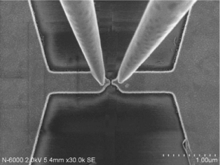
Nanogap formation & measurement example
Nano-Gap Electrode (example)
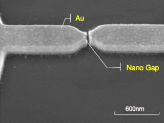
Au/Cr Electrode (gap size = 10nm)
X-SEM
Nano-Probe Measurement (example)
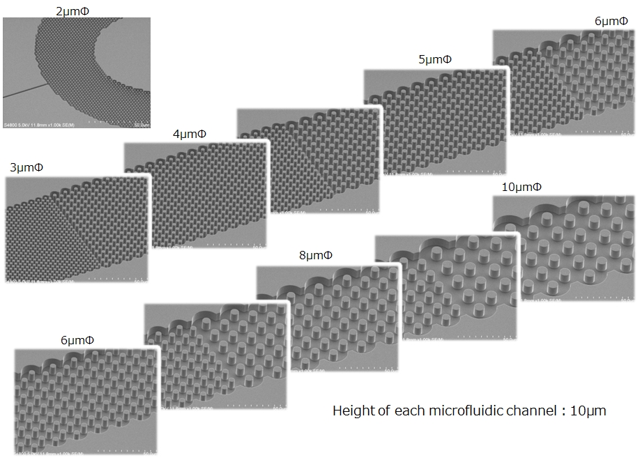
Examples of Microfluidic Channel Formation
Si pillar (example)
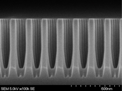
X-SEM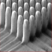
TILT SEM- Si pillar
Pitch = 140nm
Diameter = φ70±5nm
Depth = 500nm
TMAH & BHF Wet Etching Processing Services
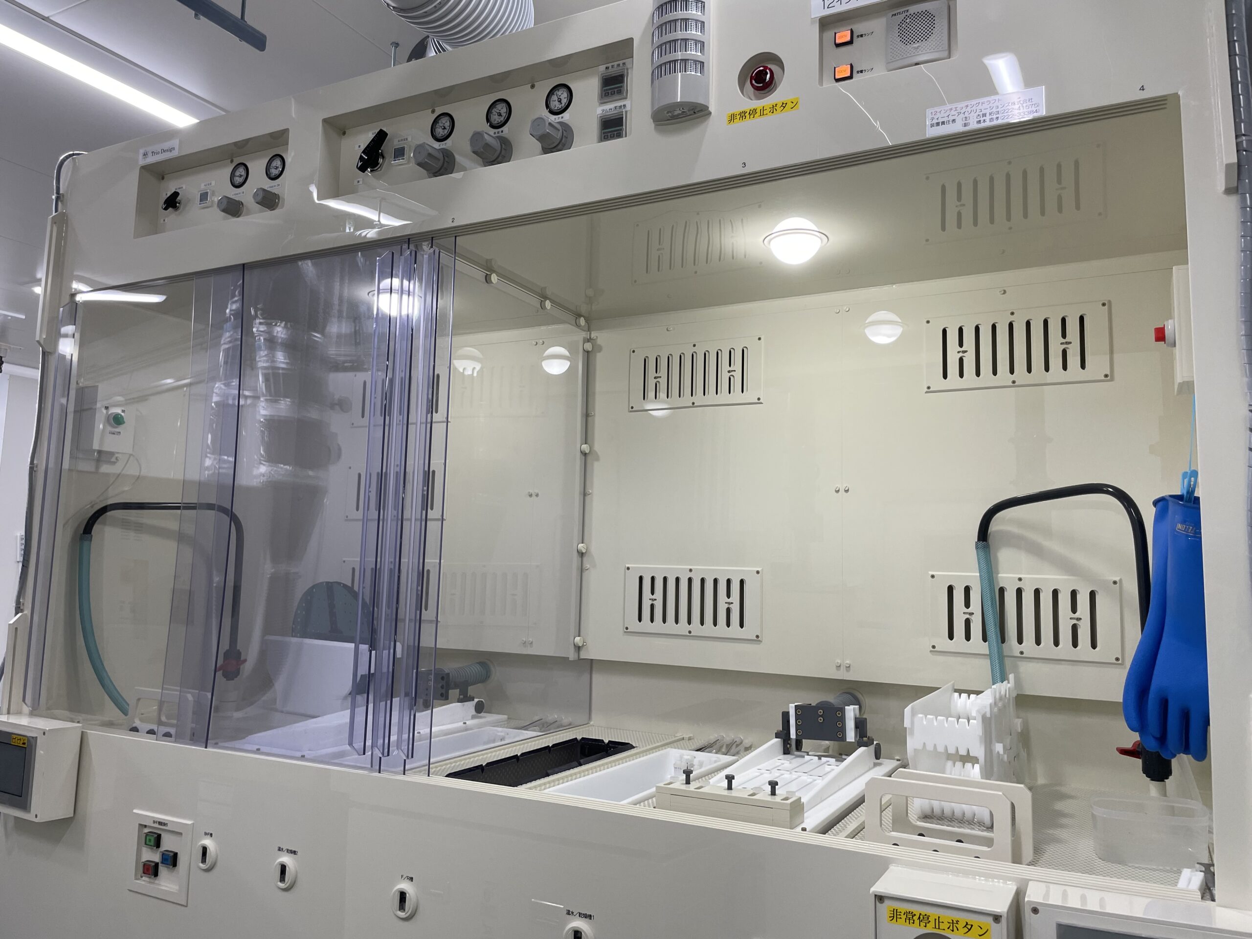
The Si etch rate for TMAH wet etching is approximately 20 μm/hour, with an in-plane uniformity of less than 10%.
Standard Theme Innovation
tei Solutions selects theme of technology development for project. Customers take part in project and share information.